Wussten Sie, dass Zellen nano-grosse Stresspusteln bekommen können? Oder wissenschaftlicher gesagt, stress granules. Und dass man deren Anzahl und Grösse und damit die Vitalität einer einzelnen lebenden Zelle mit extrem hoher Geschwindigkeit im zeitlichen Verlauf messen kann? Auch dies erfuhr man auf der diesjährigen Swiss NanoConvention in Fribourg.

Von ultraschnell geprüften Zellen zu Photonik-ICs und Quantum Computing
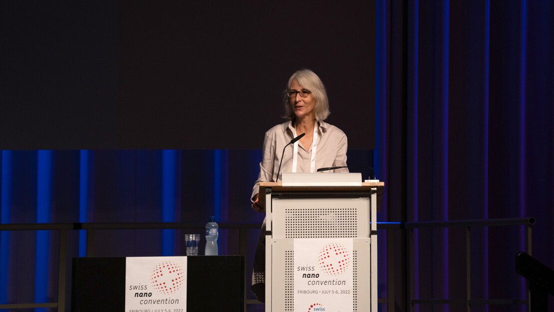
Chair Prof. Barbara Rothen, AMI, eröffnet die diesjährige Swiss NanoConvention in Fribourg. Bild: Nadine Zielinski, HTZ
Die von dem Team um die Conference Co-Chairs Barbara Rothen und Alke Fink, beide vom Freiburger Adolphe-Merkle-Institut, hervorragend organisierte Veranstaltung brachte die Schweizer Nano-Community am 5. und 6. Juli im Forum Fribourg endlich wieder in Präsenz zusammen. Die Organisatorinnen der Swiss NanoConvention 2022 zauberten zudem den Rekordwert von 38% Referentinnen auf die Bühne, wozu die Session «Highlighting Women’s Contributions in Nanoscience» ihren Teil beitrug. Zum thematischen Spektrum zählten neben den erwähnten Medtech- und Bio-Nanotechnologien vor allem zwei weitere Themenblöcke: Sogenannte PIC (photonic integrated circuits) und die Technologien hinter Quantum Computing. Begleitet wurde die SNC 2022 von der hervorragend gebuchten Ausstellung – auch mit Silber-Sponsor nano.swiss und Innovationspartner Hightech Zentrum Aargau − und einer Postersession.
Eine inspirierende Güntherodt Lecture hielt am ersten Morgen Eli Zeldov vom Weizman Institute of Science zum Thema Nanoscale thermal and magnetic imaging. Faszinierend, wie auf einer grossen Graphen-Flocke wenige einzelne atomare Defekte sichtbar gemacht werden können!
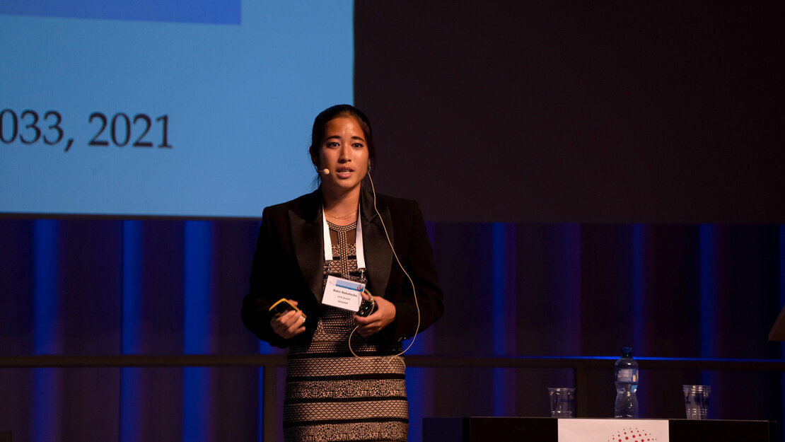
Dr. Nako Nakatsuka, Senior Scientist am Lab. of Biosensors and Bioelectronics an der ETH Zürich, spricht über «Nanoscale DNA-gated biosensors to monitor chemical flux». Bild: Nadine Zielinski, HTZ
Materialien und Anwendungen für integrierte optische Schaltkreise
PICs, integrierte aktive oder passive optische Schaltungen, ergänzen und ersetzen zunehmend «normale» ICs. Mit ihren prinzipbedingten Vorteilen werden sie immer wichtiger als Bausteine für schnellere und energieeffizientere Datenverarbeitung und -übertragung – nicht nur zwischen Datenzentren, sondern auch innerhalb dieser oder sogar auf derselben Platine.
Die Ansprüche an Geschwindigkeit und Integration wachsen, so dass derzeit mehrere Materialplattformen (Silicon-on-insulator SOI, Bariumtitanat BTO, Lithium Niobate on Insulator LNOI) und Technologien miteinander wetteifern. Um möglichst viele Funktionen auf einem optischen Chip integrieren zu können, reichen die Strukturdimensionen in die Nanoskala. Für die Fabrikation sind daher Reinräume und High-End-Oberflächentechnik ein Muss – all dies kann die Schweiz bereitstellen, bis hin zu ELENA, einer EU-geförderten open-access foundry für elektrooptische Bauteile. Sehr erfreulich dabei ist, dass Schweizer Firmen auch bei den PICs selber weltweit ganz vorne dabei sind und verschiedene ultraschnelle Schaltungen mit über 100 Gbps gezeigt werden konnten. Auch das Packaging der fertigen PIC wird immer wichtiger, wie gleich mehrere Vortragende ausführten. Erst dies erzielt den nötigen Schutz der empfindlichen Strukturen, bindet sie an externe Signalquellen, Detektoren sowie «normale» elektronische Halbleiter- und Leiterstrukturen an.
Welches ist das beste Qubit?
Ein ähnliches Rennen spielt sich bei den enorm leistungsfähigen Quantencomputern ab. Die Dimensionen gehen hier schon ins atomare, also unterhalb von 10-9 m. Verschiedene Technologien stehen zur Wahl, alle Kandidaten müssen eine Zuverlässigkeit von allermindestens 99% erreichen, damit die verfügbaren Fehlerkorrekturverfahren greifen können. Die Session «Quantum Computing» zeigte die aktuellen Ansätze basierend auf Silizium, Germanium und hybriden Halbleiter/Supraleiter-Qubits. Besonderes Augenmerk liegt auf einer zukünftigen 2D-Integrierbarkeit, die heutigen Qubits erinnern vom Volumen noch ein wenig an den ersten Transistor.
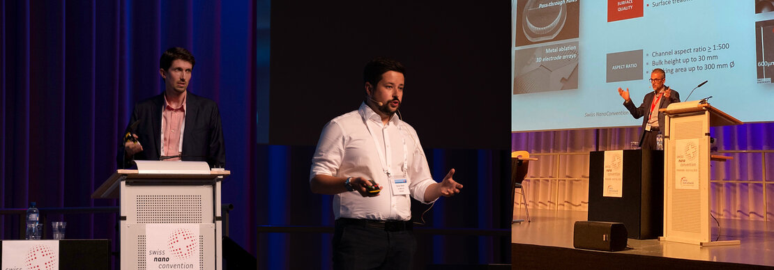
Die Referenten der Applied Session, v.l.n.r: Giole Balestra (iPrint Institut), Daniel Steitz (novoMOF AG) und Rolando Ferrini (FEMTOprint SA)
Die Industrie im Fokus
Die Industrie und die praktische Anwendung von Nanotechnologien und Nanomaterialien hatte die Session Applied Projects in the Swiss Landscape im Fokus. Chairs waren Schwerpunktleiter Werkstoff- und Nanotechnologien am HTZ, Marcus Morstein, und der Direktor der Wirtschaftsförderung Fribourg, Jerry Krattiger. Hier kam das wichtige Gebiet der additiven Fertigung zum Zug, am Beispiel von Dental-Restaurationen aus Zirkonoxid (iPrint, Giole Balestra). Dann ging es um ein echtes Nanomaterial: Metal-Organic-Frameworks (MOFs). Wie Daniel Steitz, Gründer und CIO beim Zofinger Startup novoMOF, ausführte sind diese «Nano-Schwämme» eine stark wachsende Substanzklasse mit rekordhoher spezifischer Oberfläche und immensen Potenzial zum Beispiel im Carbon Capturing. Schliesslich zeigte Rolando Ferrini (FEMTOprint SA), was man mittels laserbasiertem Advanced Manufacturing alles mit dem Material Glas anstellen kann: von Mikrofluidik-Kammern bis zu additiv gefertigten Hightech-Glaskomponenten, die erst die Anbindung der stark geschrumpften optischen Chips an die relativ dicken Lichtwellenleiter-Bündel ermöglichen. Womit wir wieder bei den PICs wären.
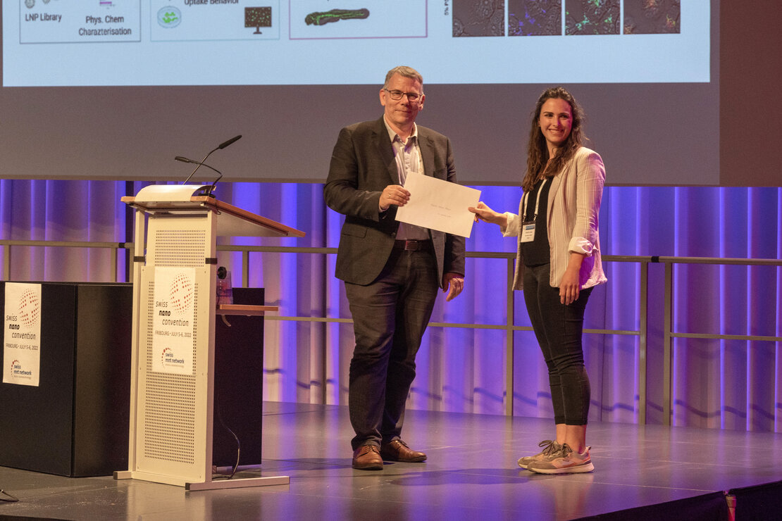
Dr. Marcus Morstein überreicht den durch das Hightech Zentrum Aargau gesponserten Ph.D. Award an Claudia Lotter. Bild: Thomas Knecht, HTZ
Der Nachwuchs ist wichtig
Zum Schluss des Programms wurden fünf Doktorandinnen und Doktoranden in der Awards Ceremony für herausragende wissenschaftliche Veröffentlichungen auf dem Gebiet der Nanotechnologien geehrt. Es war mir eine grosse Freude, für das Hightech Zentrum Aargau einen der Preise an Claudia Lotter von der Uni Basel zu überreichen. Herzlichen Glückwunsch!
Auffallend übrigens, dass viele Beiträge aus der Industrie mit einem letzten Slide endeten, auf dem eine teils eindrückliche Liste freier Stellen zu sehen war. Dies zeigt zweierlei: Fachkräfte sind nicht einfach zu finden, und Nachwuchsrekutierung kann ein zusätzlicher Grund sein, um an die SNC zu kommen.
Nächste Swiss NanoConvention in Neuchâtel
Nach der Konferenz ist vor der Konferenz: Die nächste SNC findet vom 15.-16. Juni 2023 in Neuchâtel statt. Gastgeber und Conference Co-Chairs sind Alexandra Kaempfer-Homsy (HE-ARC) und Michel Despont (CSEM). Wir freuen uns schon auf ein Wiedersehen am Neuenburger See!
(MMo / nano.swiss)
Weitere Bilder zu Swiss NanoConvention 2022:
Bildergalerie
